optimize RF PCB layout for signal integrity
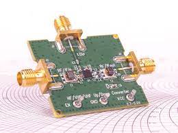
RF PCBs require special considerations in the layout stage to ensure signal integrity. This includes impedance matching, noise reduction, and decreasing signal reflections to prevent interference with other components in the circuit. In addition, minimizing the distance high-frequency signals have to travel can reduce signal loss and degradation, as well as minimize unwanted interference from external sources.
An important element of RF PCB design is the characteristic impedance (Z0) of each transmission line, which represents the resistance and capacitance of the line when a voltage wave passes through it. It is determined by the physical dimensions and properties of the line, including its width, thickness, dielectric material, and relative permittivity. Ideally, the Z0 of each transmission line should match the impedance of its source and load to reduce signal reflections and maximize power transfer. This requires careful calculations, especially in the case of curved traces that can have complex impedance characteristics.
The loss tangent of an rf pcb is another significant factor in its performance. This metric is used to determine how much energy the PCB’s components and traces dissipate during operation. The lower the tangent value, the better. However, calculating the loss tangent of an RF PCB can be difficult since the material properties are not usually known in detail. Therefore, it is often necessary to use a field solver to evaluate a design for RF performance.
How do you optimize RF PCB layout for signal integrity?
Trace length and vias are also critical factors in RF performance. RF signals must travel long distances to reach their destination, which increases the chance of loss and interference. This can be minimized by keeping the trace length as short as possible and using smaller vias with high dielectric constants to reduce losses.
Another major concern in RF design is reducing the amount of noise that is generated by the power supply. This can be done by employing decoupling capacitors to filter out the noise. This is accomplished by connecting the capacitors with minimum impedance, preferably in parallel with each other.
To further decrease noise, a ground plane is placed near the RF layer to create a low-impedance return path for signals. This can be further enhanced by placing decoupling capacitors close to the power and ground pins of each component to reduce noise generated by these connections.
RF circuits must be protected from outside interference by shielding and other techniques. It is also crucial to test and optimize RF PCB layouts before prototyping, as this can help avoid problems and improve performance. Once a prototype has been tested and optimized, the final RF PCB can be designed to meet its specific application. The end result is a highly reliable and functional RF circuit that can perform as intended. To do this, it is important to follow RF PCB layout guidelines, use proper simulation tools, and understand the behavior of high-frequency signals. With these methods, the design and layout process can be made more efficient while maintaining a high level of quality.