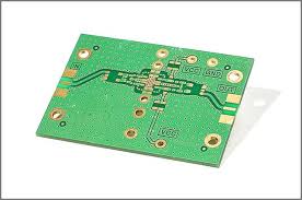
advantages of using rf circuit boards
RF circuit boards are an integral part of modern technologies like cellular, GPS, radar, and wireless communication systems. They facilitate the wireless transfer of high-frequency signals between devices using various protocols like Bluetooth, ZigBee, RFID, cellular, and LoRa. They can operate from hundreds of MHz to tens of GHz, supporting the major wireless bands used in modern communications, radar, and other applications. RF PCBs feature various features to ensure signal integrity, including impedance matching, noise reduction, and shielding structures.
Choosing the right materials for a RF circuit board is crucial to its performance. RF PCBs typically use polytetrafl uoroethylene (PTFE) and ceramics mixed with hydrocarbons and different forms of glass. These materials are known as Rogers laminates and offer superior electrical properties compared to conventional organic substrates such as FR-4. Using these materials reduces insertion loss and impedance variation and allows the use of shorter trace lengths, which in turn improves signal transmission efficiency and performance.
The choice of a rf circuit board layout also affects its performance. The layout must include careful routing of the RF signal and power lines to prevent interference with digital components or other traces. This can be done through the use of ground planes, guard traces, and distance separation between the RF circuit and noisy digital components. It is also important to use the correct via diameter and aspect ratio to reduce via inductance.

What are the advantages of using rf circuit boards?
Another factor that contributes to signal degradation is crosstalk. Crosstalk occurs when RF traces interfere with each other, causing a loss of signal strength. To mitigate this, RF designers must route traces that are as straight point-to-point as possible and avoid 90-degree bends. They should also minimize the number of layers between traces to avoid coupling.
In addition to the design factors mentioned above, RF circuit boards must be designed with precision in layer alignment and etching. This is because any misalignment can cause impedance mismatches, which negatively impact RF performance. The use of simulation tools can help prevent such problems by allowing designers to test their designs virtually, adjusting tracing widths and spacings, modifying RF PCB stack-ups, and repositioning components to optimize the design for performance before fabrication.
It is also critical to consider the thermal properties of RF PCBs when designing a multilayer layout. The soldering process generates considerable heat, which can cause extensive thermal stress in the layers of the multilayer RF circuit board. To compensate for this, a suitable material with a low coefficient of thermal expansion must be selected. This will help to maintain registration alignment of the layers during manufacturing and reduce thermal stresses after assembly. A layered PCB can also benefit from the use of conductive foils to separate layers and improve signal transmission. In addition, it is helpful to choose a PCB material with a low dielectric constant (Dk) that can support the circuit’s impedance and frequency range. For example, a woven glass-reinforced PTFE laminate has a Dk of 6.8 and is well suited for microstrip circuits.